- 您现在的位置:买卖IC网 > Sheet目录471 > MAX19700EVKIT (Maxim Integrated)EVAL KIT FOR MAX19700
�� �
�
�MAX19700� Evaluation� Kit/Evaluation� System�
�Reference�
�The� MAX19700� features� two� reference� operation�
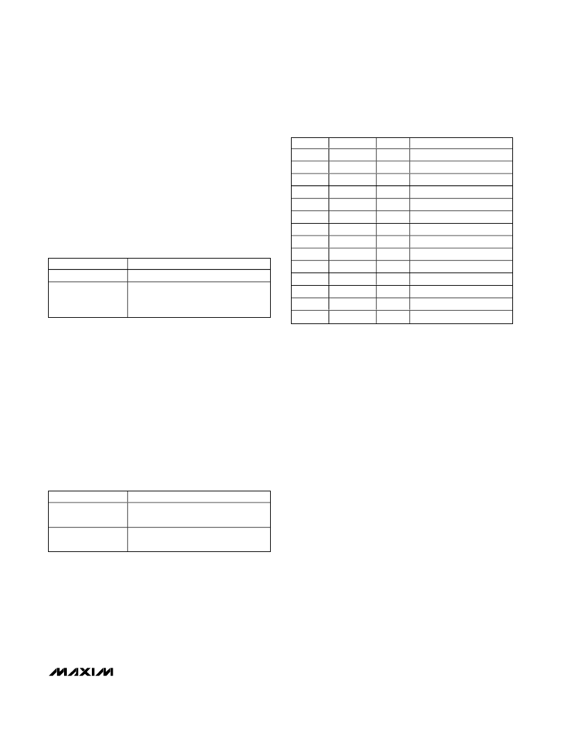
�Table� 5.� Digital� Data� Bit� Locations�
�modes.� The� EV� kit� can� be� configured� to� use� either� the�
�SIGNAL� LOCATION�
�TYPE�
�DESCRIPTION�
�MAX19700� internal� (1.024V)� reference� or� an� external�
�user-supplied� reference� applied� at� the� REFIN� pad.� The�
�MAX19700� generates� the� REFP� and� REFN� voltages�
�from� the� selected� reference� voltage� (refer� to� the�
�MAX19700� data� sheet� for� more� details).� Measure� the�
�REFP� and� REFN� voltages� at� TP1� and� TP2,� respectively.�
�Jumper� JU4� controls� the� reference� mode.� See� Table� 3�
�for� jumper� configuration.�
�Table� 3.� Reference� Shunt� Settings� (JU4)�
�D0�
�D1�
�D2�
�D3�
�D4�
�D5�
�D6�
�D7�
�D8�
�J11-37�
�J11-35�
�J11-33�
�J11-31�
�J11-29�
�J11-27�
�J11-25�
�J11-23�
�J11-21�
�I/O�
�I/O�
�I/O�
�I/O�
�I/O�
�I/O�
�I/O�
�I/O�
�I/O�
�Data� Bit� 0� (LSB)�
�Data� Bit� 1�
�Data� Bit� 2�
�Data� Bit� 3�
�Data� Bit� 4�
�Data� Bit� 5�
�Data� Bit� 6�
�Data� Bit� 7�
�Data� Bit� 8�
�SHUNT� POSITION�
�Installed*�
�Not� installed�
�DESCRIPTION�
�Internal� reference� mode�
�External� reference� mode� —� apply� an�
�external� reference� voltage� to� the� REFIN�
�pad�
�D9�
�SHDN�
�Tx/� Rx�
�DR�
�CLK�
�J11-19�
�J11-13�
�J11-9�
�J11-3�
�J11-1�
�I/O�
�I/O**�
�I/O**�
�Output�
�Output�
�Data� Bit� 9� (MSB)�
�Shutdown� Status**�
�Transmit/Receive� Status**�
�Data-Ready� Signal�
�Incoming� Clock� Signal�
�*� Default� configuration:� JU4� (installed).�
�Digital� Data� Header�
�The� MAX19700� features� one� 10-bit� parallel,� bidirection-�
�al� data� bus� that� transmits/receives� the� converted� ana-�
�log� signals.� Refer� to� the� MAX19700� data� sheet� for� more�
�details.�
�Digital� Data� Direction�
�The� MAX19700� EV� kit� features� an� on-board,� bidirection-�
�al,� level-translating� buffer� in� the� parallel� digital� data�
�path.� Jumper� JU3� controls� the� direction� of� the� data�
�bus.� See� Table� 4� for� jumper� configuration.�
�Table� 4.� Output� Format� Shunt� Settings�
�(JU3)�
�**� SHDN� and� Tx/� Rx� default� to� outputs,� but� can� be� configured� to�
�inputs.� See� the� Configuring� for� ASIC/FPGA� Connection� section�
�in� this� document.�
�Note:� All� signal� directions� are� with� respect� to� the� EV� kit.� Pins� 5,�
�7,� 11,� 15,� 17,� 39,� and� 40� of� J11� are� open.� All� other� pins� are�
�connected� to� DGND.�
�Configuring� for� ASIC/FPGA� Connection�
�The� MAX19700� EV� kit� is� designed� to� be� connected� to�
�an� ASIC� or� FPGA.� To� complete� this� connection,� follow�
�the� list� of� instructions� below:�
�1)� Remove� the� shunt� from� jumper� JU2.�
�2)� Remove� the� shunt� from� jumper� JU3.�
�3)� Connect� ASIC/FPGA� to� header� J11� (see� the� Digital�
�Data� Bit� Locations� section� in� this� document� for�
�SHUNT� POSITION�
�1-2�
�2-3*�
�DESCRIPTION�
�Transmit� path� enabled;� D0� –� D9� are�
�inputs�
�Receive� path� enabled;� D0� –� D9� are�
�outputs�
�header� connections).�
�4)� Ensure� that� the� voltage� at� BVCC� matches� the�
�ASIC/FPGA� I/O� voltage.�
�The� ASIC/FPGA� must� control� all� signals� connected� to�
�the� MAX19700,� including� SHDN� and� Tx/� Rx� .�
�*� Default� configuration:� JU3� (2-3).�
�Digital� Data� Bit� Locations�
�A� driver� (U2)� buffers� the� digital� I/Os� of� the� MAX19700.�
�This� driver� is� able� to� drive� large� capacitive� loads,� which�
�may� be� present� at� the� logic� analyzer� connection.� The�
�outputs� of� the� buffer� are� connected� to� a� 40-pin� header�
�(J11).� See� Table� 5� for� bit� locations� on� header� J11.�
�_______________________________________________________________________________________�
�9�
�发布紧急采购,3分钟左右您将得到回复。
相关PDF资料
MAX19985AETX+T
IC MIXER DOWNCONV 36-TQFN-EP
MAX19993ETX+
IC MIXER DOWNCONV 36TQFN
MAX19994AEVKIT#
KIT EVAL FOR MAX19994A MIXER
MAX19995ETX+T
IC DOWNCONVERTER 2CH 36TQFN
MAX19995EVKIT#
EVALUATION KIT FOR MAX19995
MAX19996AEVKIT#
EVALUATION KIT FOR MAX19996A
MAX19996ETP+T
IC MIXER DOWNCONV 20-TQFN-EP
MAX19997AETX+T
IC DOWNCONVERTER 2CH 36TQFN
相关代理商/技术参数
MAX19705ETM
功能描述:ADC / DAC多通道 RoHS:否 制造商:Texas Instruments 转换速率: 分辨率:8 bit 接口类型:SPI 电压参考: 电源电压-最大:3.6 V 电源电压-最小:2 V 最大工作温度:+ 85 C 安装风格:SMD/SMT 封装 / 箱体:VQFN-40
MAX19705ETM+
功能描述:ADC / DAC多通道 7.5Msps CODEC/AFE 1.8/2.7-3.3V RoHS:否 制造商:Texas Instruments 转换速率: 分辨率:8 bit 接口类型:SPI 电压参考: 电源电压-最大:3.6 V 电源电压-最小:2 V 最大工作温度:+ 85 C 安装风格:SMD/SMT 封装 / 箱体:VQFN-40
MAX19705ETM+GH7
功能描述:ADC / DAC多通道 10-Bit 7.5Msps Ultra-Low-Power Analog Front-End RoHS:否 制造商:Texas Instruments 转换速率: 分辨率:8 bit 接口类型:SPI 电压参考: 电源电压-最大:3.6 V 电源电压-最小:2 V 最大工作温度:+ 85 C 安装风格:SMD/SMT 封装 / 箱体:VQFN-40
MAX19705ETM+T
功能描述:ADC / DAC多通道 7.5Msps CODEC/AFE 1.8/2.7-3.3V RoHS:否 制造商:Texas Instruments 转换速率: 分辨率:8 bit 接口类型:SPI 电压参考: 电源电压-最大:3.6 V 电源电压-最小:2 V 最大工作温度:+ 85 C 安装风格:SMD/SMT 封装 / 箱体:VQFN-40
MAX19705ETM+TGH7
功能描述:ADC / DAC多通道 10-bit 7.5Msps Ultra-Low-Power Analog Front-End RoHS:否 制造商:Texas Instruments 转换速率: 分辨率:8 bit 接口类型:SPI 电压参考: 电源电压-最大:3.6 V 电源电压-最小:2 V 最大工作温度:+ 85 C 安装风格:SMD/SMT 封装 / 箱体:VQFN-40
MAX19705ETM-T
功能描述:ADC / DAC多通道 RoHS:否 制造商:Texas Instruments 转换速率: 分辨率:8 bit 接口类型:SPI 电压参考: 电源电压-最大:3.6 V 电源电压-最小:2 V 最大工作温度:+ 85 C 安装风格:SMD/SMT 封装 / 箱体:VQFN-40
MAX19705EVCMOD2
功能描述:ADC / DAC多通道 Evaluation System for the MAX19705 RoHS:否 制造商:Texas Instruments 转换速率: 分辨率:8 bit 接口类型:SPI 电压参考: 电源电压-最大:3.6 V 电源电压-最小:2 V 最大工作温度:+ 85 C 安装风格:SMD/SMT 封装 / 箱体:VQFN-40
MAX19705EVCMODU
功能描述:ADC / DAC多通道 Evaluation System for the MAX19705 RoHS:否 制造商:Texas Instruments 转换速率: 分辨率:8 bit 接口类型:SPI 电压参考: 电源电压-最大:3.6 V 电源电压-最小:2 V 最大工作温度:+ 85 C 安装风格:SMD/SMT 封装 / 箱体:VQFN-40